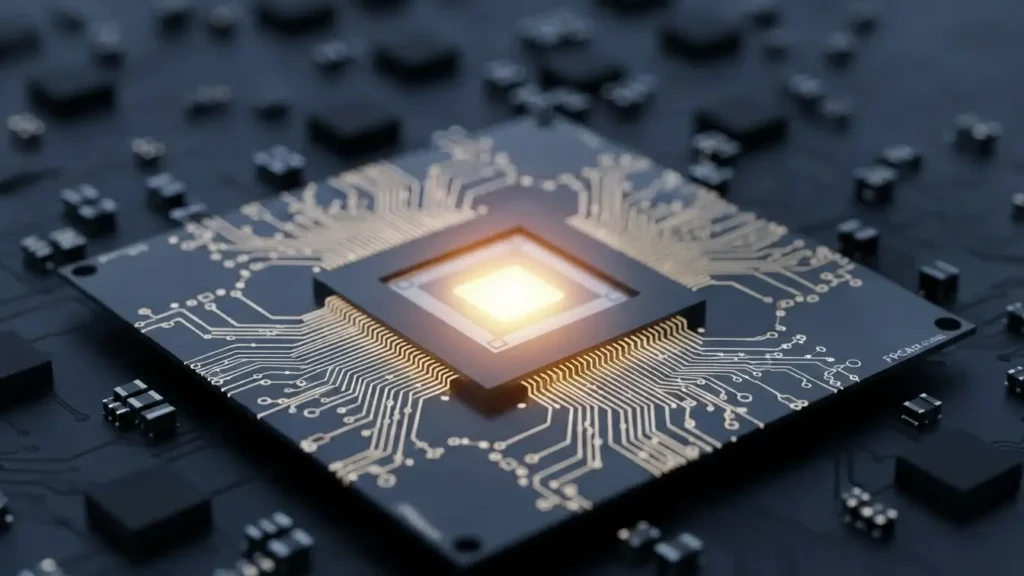
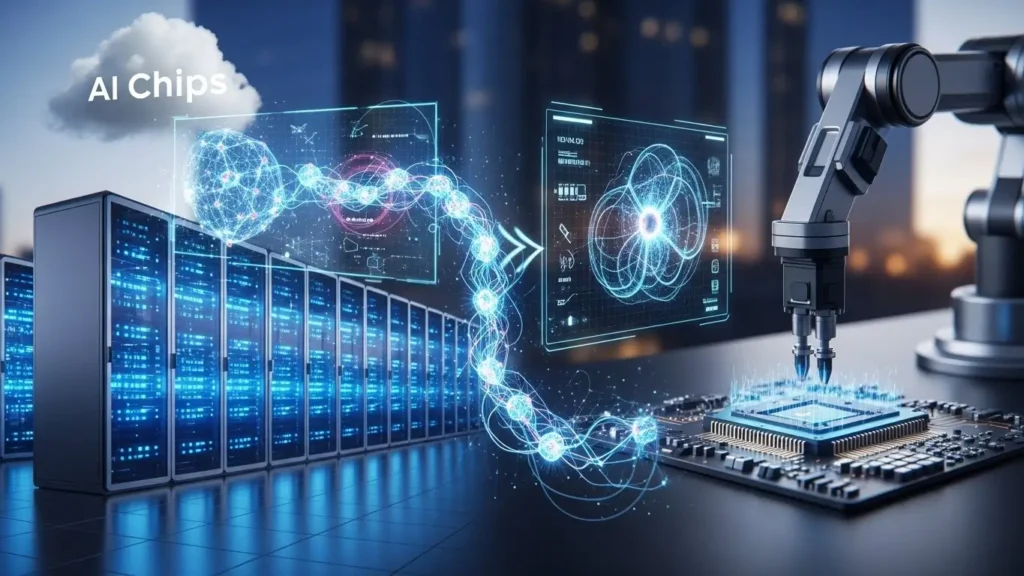
The revolution in artificial intelligence is fundamentally a revolution in silicon. Discover the high-stakes, multi-billion-dollar war being waged for control of the hardware that powers everything from massive language models to the AI on your smartphone. Our comprehensive report, based on expert analysis, dissects the complex landscape of ai chips for the future, offering an unprecedented look into the strategies, technologies and geopolitics driving this crucial industry.
For years, Nvidia’s GPUs dominated the landscape, serving as the general-purpose workhorse for generative AI training. But a fundamental shift is underway: the world’s largest cloud providers Google, Amazon and Microsoft are aggressively moving to custom ai chips (ASICs). These specialized accelerators, such as the Tensor Processing Unit (TPU) and Trainium, are more power-efficient, cost-effective and provide the performance needed for the soaring demand of AI inference. Learn why this vertical integration strategy is critical for hyperscalers seeking to cut costs and reduce reliance on a single external supplier.
The competition extends far beyond the data center. The rise of Edge AI, powered by Neural Processing Units (NPUs) and FPGAs, is shrinking intelligence onto low-power ai chips for the future integrated into laptops, cars and smart devices. Crucially, this article unpacks the major geopolitical constraint: the concentration of advanced manufacturing in Taiwan. With the US CHIPS Act funding a massive reshoring effort by TSMC and Intel, we analyze how the supply chain battle is bringing the silicon back to American shores while addressing the critical challenge of AI’s massive energy consumption. This is the definitive guide to understanding the next era of computing.
The Undisputed King: Why GPUs Became the Blueprint for AI Acceleration
The initial catalyst for the modern AI boom was the Graphics Processing Unit (GPU). Once the domain of gamers looking for hyper-realistic graphics, the GPU quickly became the heart of deep learning.

The Birth of AI Computing: Parallelism and AlexNet
To grasp the central role of the GPU, we must understand its architecture. Unlike a Central Processing Unit (CPU), which features a few powerful cores designed to run sequential, general-purpose tasks, the GPU is built for parallel processing. It contains thousands of smaller, more narrowly focused cores. This structure was purpose-built to render images: when generating a lifelike scene, a computer needs to calculate the light, color and texture of millions of pixels simultaneously.
In 2012, this inherent capability found its true calling in artificial intelligence. Researchers, in what is often considered AI’s big bang moment, introduced AlexNet, an incredibly accurate neural network. They realized the same parallel computational capabilities that rendered lifelike graphics could be “hacked” to unlock massive performance for deep learning. Neural networks learn by processing multidimensional data structures known as tensors a task perfectly suited to the GPU’s thousands of parallel math units, often called matrix multiplication engines.
The result: Nvidia, the pioneer of the GPU, catapulted from a gaming giant to the very core of generative AI. Today, the latest Nvidia AI chips, such as the Blackwell GPUs, are inside server racks globally, training the foundational models and running the demanding workloads that power the digital world. Their latest systems, like the 72-GPU Blackwell server rack, sell for around $3 million, with Nvidia reportedly shipping thousands each week. This system-level approach selling the entire rack, not just the chip highlights Nvidia’s focus on providing a complete, highly efficient compute solution to secure its dominance in the market for ai chips for the future.
The Power of CUDA: Nvidia’s Moat
Nvidia’s success is not just about raw silicon performance; it is equally dependent on its proprietary software platform, CUDA. CUDA is the comprehensive software ecosystem that underpins nearly all major AI frameworks PyTorch, TensorFlow, and JAX making it the universal language for AI researchers and developers worldwide. This mature tooling and accessibility have established a massive developer ecosystem around Nvidia’s architecture. Once developers build their models around CUDA, switching to a competitor’s hardware, like Google’s tensor processing unit (tpu) or AMD’s Instinct GPU line, involves significant costs and refactoring of code, securing Nvidia’s position at the apex of ai chips for the future.
Nvidia’s top competitor, Advanced Micro Devices (AMD), with its Instinct GPUs, is gaining traction, especially with major commitments from key players like OpenAI and Oracle. A key differentiator is that AMD favors a largely open-source software ecosystem, offering an alternative to Nvidia’s locked-down environment. This competition is crucial for driving innovation and offering developers more choice in AI accelerator chips.
Training vs. Inference: The Critical Divide in AI Workloads
Not all AI tasks are created equal. The AI computation workflow is fundamentally split into two distinct phases, each requiring different chip characteristics: training and inference. Understanding this divide is paramount to grasping the competitive landscape of custom ai chips and general-purpose GPUs.
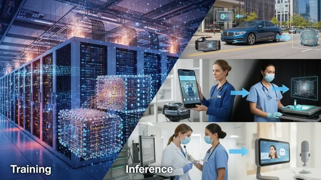
Training: The Compute-Intensive Phase
Training is the initial and most compute-intensive phase. It involves teaching the AI model to learn from patterns hidden within vast amounts of data, often requiring weeks or months of continuous, massive-scale parallel computation. This stage is a perfect job for powerful, flexible, high-capacity GPUs and it’s why specialized AI chips for training remain in such high demand globally.
Inference: The Everyday Application Phase
Inference, conversely, is when the trained AI model is put to work to make decisions or predictions based on new information. This is how AI shows up in everyday applications: the chatbot you interact with, the recommendation engine on your shopping app or the language model powering your EarPods. This phase requires rapid, low-latency processing and often happens repeatedly billions of times a day. As Large Language Models (LLMs) mature, the demand for inference capacity is surging far faster than the need for initial training. This massive shift in workload emphasis is opening the door for new types of hardware.
Inference can happen on less powerful chips programed for more specific tasks, creating a strategic opening for highly efficient, cost-optimized custom ai chips.
The Vertical Integration Strategy: The Rise of Custom AI Chips
The immense cost, high power consumption and supply-chain reliance on Nvidia’s high-end GPUs have driven the world’s largest cloud providers Google, Amazon, Meta and Microsoft to invest heavily in developing their own application specific integrated circuit (ASIC) designs. This movement toward custom silicon represents a strategic power play to gain greater control over costs, performance and infrastructure efficiency.
Custom ASICs: The Single-Purpose Powerhouse
If a GPU is a Swiss Army knife flexible enough to handle many kinds of parallel math for different AI workloads an ASIC is a single-purpose, highly refined tool. It is hardwired into silicon to perform the exact math for one type of job, making it much, much more efficient and faster for that specific task.
While designing a Custom AI Chip is hugely expensive, costing minimum tens and often hundreds, of millions of dollars the long-term benefits for a hyperscaler are undeniable:
- Cost Reduction: ASICs are more power-efficient than general-purpose GPUs, significantly driving down the operational cost of running AI services at scale. Cloud providers need to bring the cost of AI down to maintain profitability.
- Performance Optimization: Chips can be precisely tuned to the unique workloads of the cloud provider’s services (e.g., Google Search, Amazon’s recommendation engines), yielding a better performance-per-watt ratio.
- Supply Control: Reduces critical reliance on a single third-party supplier, Nvidia, giving the cloud provider more control over the supply chain and pricing.
Google’s Tensor Processing Unit (TPU): The Trailblazer
Google was the first to make a custom ASIC for AI acceleration, coining the term tensor processing unit (TPU) when its first ASIC came out in 2015. This groundbreaking work also helped lead to the invention of the transformer in 2017 the foundational architecture powering almost all modern AI, including LLMs like Google’s Gemini and Anthropic’s Claude.
A decade later, Google has released its seventh generation, codenamed Ironwood (Trillium), which features colorful cables linking all of the chips to work as one large supercomputer. While Google has traditionally used TPUs primarily for in-house purposes powering services like Google Search and Translate there is increasing speculation that the company will open up access to TPUs more broadly to compete directly with Nvidia in the market for ai chips for the future.
In a major validation of this technology, Anthropic has committed to training its Claude LLM on up to a million TPUs. Some experts even believe that the TPU architecture, optimized for scale and efficiency, is technically on par or even superior to Nvidia’s for specific LLM workloads.
Amazon’s Trainium and Inferentia: The Price-Performance Champions
Amazon Web Services (AWS) followed Google, launching its own custom AI chips for cloud services after acquiring Annapurna Labs in 2015. AWS offers a dual-chip strategy: Inferentia (optimized for inference) and Trainium (optimized for training).
AWS has aggressively marketed these chips based on price performance. The company has stated that AWS Trainium provides between 30% and 40% better price performance compared to other hardware vendors in AWS for training large language models. The architecture of a Trainium cluster is often described as a series of flexible workshops, contrasting with the more rigid, centralized grid of Google’s TPU. This difference in design highlights the diverse approaches to solving parallel math problems in ai chips for the future.
Amazon demonstrated its commitment to its custom silicon by revealing its biggest AI data center, where Anthropic is training its models on half-a-million Trainium2 chips a massive deployment that contains no Nvidia GPUs. However, reflecting the dual strategy of the cloud giants, AWS continues to fill its other data centers with copious amounts of Nvidia GPUs to meet the massive, varied demand from its AI customers, highlighting the sustained need for general-purpose compute alongside specialized chips.
The Ecosystem of Innovation: Custom Silicon Beyond the Giants
The revolution in custom ai chips is not solely a two-way street between the hyperscalers and Nvidia. It involves a sophisticated ecosystem of specialist partners, ambitious rivals and focused startups, all driving the evolution of ai chips for the future. The core of this expansion is the desire for optimization, efficiency and architectural diversity in a market previously dominated by general-purpose hardware.
The Architects Behind the ASICs: Broadcom, Marvell and OpenAI
The massive undertaking of designing and building application specific integrated circuits is often too complex and costly for even tech giants to handle entirely in-house. This difficulty has created a significant boom for backend partners like Broadcom and Marvell. These companies provide the critical Intellectual Property (IP), design know-how and high-speed networking components essential for linking thousands of custom ai chips into a massive ai chips for data centers supercomputer.
Broadcom in particular has emerged as one of the biggest beneficiaries of the AI boom, securing a dominant position in the market. It helped build Google’s groundbreaking TPUs and Meta’s training and inference accelerators. Most notably, Broadcom secured a colossal deal to help OpenAI a massive consumer of Nvidia GPUs develop its own custom ASICs starting in 2026. This move by OpenAI is perhaps the clearest signal that even the most well-funded AI research labs see the strategic necessity of vertical integration and optimization in their quest for the most efficient ai chips for the future. Analysts predict Broadcom could win 70% to 80% of this specialized market, demonstrating the accelerating pace of ai chip design.
The Contenders: Microsoft, Intel and the Startups
Beyond the major cloud providers, several other high-profile technology companies and dynamic startups are aggressively pushing their own custom ai chips into the marketplace, creating intense competition in ai chips news.
- Microsoft’s Maia: Microsoft is developing its Maia chips primarily for use within its own Azure data centers. The strategy mirrors that of Google and Amazon: reduce costs, control the silicon roadmap and offer highly optimized hardware for its specific AI infrastructure. Although its next-generation chip has faced delays, the commitment of Microsoft underscores the long-term trend toward internal custom silicon.
- Intel’s Gaudi: Intel, the traditional CPU behemoth, is leveraging its Gaudi line of ai accelerator chips. Intel is aggressively reviving its foundry business the chip manufacturing arm to compete with global leaders, positioning itself as a full-service provider that can both design and manufacture advanced silicon, including its own intel ai chips.
- The Innovators (Tesla, Qualcomm, Startups): Tesla has announced its own ASIC for optimizing its autonomy software, underscoring the demand for ai chips for autonomous vehicles. Qualcomm, the leader in mobile processors, is breaking into the data center market with its AI200 to compete in the enterprise space. Meanwhile, startups like Cerebras are pioneering massive, wafer-scale ai chips that push the physical boundaries of parallel computation, and Grok is focusing on inference with specialized Language Processing Units (LPUs). These ai chips companies are all contributing to the diversification of the ai hardware chips landscape.
Shrinking AI: The Rise of Edge Computing and NPUs
While the data center currently receives the majority of funding and attention, the future of ai chips is also decidedly distributed, moving out of the cloud and onto personal devices. This is the realm of Edge AI running models locally on a device like a phone, laptop or car, instead of communicating back to a distant data center.

Why On-Device AI is Critical for the Future
On-device AI offers three significant advantages that are driving the development of ai chips for edge devices:
- Privacy and Security: By processing data locally, sensitive information never leaves the personal device, vastly improving user privacy.
- Responsiveness and Efficiency: Eliminating the need for network communication (latency) makes AI features faster and more responsive, while reducing the energy consumption associated with constantly transferring data to the cloud.
- Cost: Reduces the cloud compute burden on service providers.
NPUs and SoCs: The New Mobile Brains
The dominant technology driving this shift is the Neural Processing Unit (NPU). The NPU is a dedicated ai accelerator chip integrated directly into the device’s main processor, known as a System on a Chip (SoC). An SoC combines many different modules CPU, GPU, memory controller and now the NPU onto a single piece of silicon to create a compressed, power-efficient system capable of doing many things, crucial for ai chips for smartphones and laptops.
- Smartphones and Laptops: Qualcomm ai chips, intel ai chips and AMD ai chips are the primary drivers of NPUs enabling AI in PCs. Apple, a leader in vertical integration, includes a dedicated Neural Engine within its in-house M-series and iPhone A-series chips. These low power ai chips are enabling features like real-time language translation, advanced photography and personalized assistance directly on the device.
- Automotive and IoT: Edge AI chips companies like NXP and Nvidia are building accelerators for cars, robots, cameras and smart home devices. This deployment of ai chips for robotics and ai chips for autonomous vehicles ensures that critical real-time decisions, such as those related to safety and navigation, can be made instantly without relying on cloud connectivity. The focus will broaden significantly from the data center to include all these edge applications.
FPGAs: The Flexibility Middle Ground
The final category of specialized hardware critical to the ai chips for the future discussion are Field Programmable Gate Arrays, or FPGAs. While not as dominant as GPUs or ASICs, FPGAs provide a critical architectural bridge between general-purpose flexibility and application-specific efficiency.
The Reconfigurable Silicon
FPGAs are unique because they can be reconfigured with software after they have been manufactured. This inherent flexibility allows them to be used in diverse applications, from networking and signal processing to niche AI workloads. A user would choose an fpga for ai because they desire high performance and efficiency gains over a GPU, but do not want to incur the enormous expense, time and risk involved in designing a custom ASIC.
However, this flexibility comes at a cost: FPGAs typically offer lower raw performance and suffer from lower energy efficiency compared to a rigid, hardwired ASIC for the same specific ai chips for machine learning task. Ultimately, for the massive scale operations of hyperscalers, ASICs are cheaper when thousands of units are required.
The FPGA Titans: AMD and Intel
The competition in the FPGA space is primarily between two established semiconductor giants:
- AMD, which became the largest FPGA maker after its massive acquisition of Xilinx.
- Intel, which secured the second-place position after acquiring Altera.
This strategic competition, though quieter than the GPU vs. ASIC war, ensures that the semiconductor market continues to offer options across the entire spectrum of flexibility and specialization, cementing their role in the complete ai chips ecosystem.
The Manufacturing Bottleneck: Geopolitics and the AI Chips Supply Chain
The revolution in ai chips for the future is not merely a design battle it is a manufacturing challenge that touches on global politics, national security and economic resilience. The immense complexity and capital required to produce the most advanced silicon nodes have led to a dangerous concentration of manufacturing power.

The Taiwan Factor: A Geopolitical Issue
Today, the giants like Nvidia, Google and Amazon rely almost entirely on a single company to manufacture their cutting-edge chips: the Taiwan Semiconductor Manufacturing Company (TSMC). For years, the advanced ai chip fabs required to produce transistors at the three and four nanometer scale have been concentrated overwhelmingly in Taiwan. As an AI and semiconductor policy advisor for the Biden administration noted, this concentration has become a significant geopolitical issue in the semiconductor industry.
The world’s dependence on Taiwan for the production of sophisticated ai chips for the future creates a single point of failure and strategic vulnerability. For instance, while Apple has committed to moving some chip production to the TSMC Arizona plant, its latest high-end processors are still made using TSMC’s three-nanometer node, currently only possible in Taiwan. Even Nvidia’s powerful Blackwell architecture is manufactured using TSMC’s four-nanometer node, highlighting the dependency even for the most dominant player in ai chips news.
Reshoring the Silicon: The US Foundry Revival
In response to these supply chain risks, the US government passed the CHIPS Act, aiming to revitalize domestic chip manufacturing and ensure the US stays globally competitive in the race for advanced silicon. This strategic investment is driving a significant reshoring effort.
Intel has aggressively revived its foundry business, investing heavily in building advanced node ai chip fabs in Arizona capable of producing cutting-edge 18-angstrom chips. Simultaneously, TSMC has committed to bringing high-volume manufacturing to its giant new chip fabrication plant in Arizona. The commitment from these key ai chip manufacturers, supported by major government incentives, marks a concerted effort to bring the advanced ai chips supply chain back to American soil.
As one expert put it, ai chips for the future might very well be bringing the silicon back to Silicon Valley by creating an incredible opportunity to leverage physical AI and advanced manufacturing capabilities here in the ai chips trends USA. This ai chips investment is about more than just chip production; it’s about securing America’s technological leadership and advancing national security goals.
The Critical Constraints: Energy and Global Rivalry
Beyond the silicon and the supply chain, two major factors threaten to constrain the relentless growth of the AI chips market size: energy consumption and geopolitical rivalry.

The Hidden Cost: AI Chips Energy Consumption
The training and deployment of massive foundation models require staggering amounts of electricity. This massive AI chips energy consumption is necessary to run the hyperscale data centers that house millions of GPUs and custom ai chips. If the US is to continue leading the AI race, the national capacity to build out clean, reliable energy infrastructure is critical. China, for instance, has been noted for handling this energy build-out more effectively than the US in some areas, highlighting a major energy risk.
The push toward more efficient hardware specifically the development of low power ai chips and specialized ASICs is directly tied to the need for ai chips energy efficiency. Whether it’s optimizing ai chips for edge computing or developing sustainable ai chips for massive ai chips for data centers, the ability to secure enough power and manage the environmental impact remains a critical differentiator that will shape the future of ai chips.
Global Rivals and Export Controls
The US competition for ai chips for the future is not limited to domestic players. Major Chinese tech giants, including Huawei, ByteDance and Alibaba, are actively designing their own custom ai chips and ASICs. They recognize the necessity of internal silicon development for national strategic advantage.
However, these Chinese players are significantly limited by US export controls that restrict their access to the most advanced chip-making equipment (from companies like ASML) and the most advanced Nvidia AI chips like Blackwell. These controls are designed to maintain a multi-generational technical lead for the US and its allies. The resulting pressure forces Chinese companies to innovate within constrained technological parameters, creating a two-tiered system for ai chips performance benchmark. Despite the limitations, the global race for ai chip design tools and cutting-edge ai chip innovations ensures the competition remains intense.
Conclusion: The Dual Future of AI Chips
The era of monolithic GPU dominance is giving way to a more complex, specialized and highly competitive landscape. Nvidia’s lead is formidable; they’ve earned their position by building an entrenched, high-performance platform and winning the crucial developer ecosystem through CUDA. Dethroning the most valuable company in the world won’t come easily, but the market is becoming so vast with mid double-digit CAGR expected over the next five years that it guarantees the continued entry of new competitors.
The AI chips market forecast points to a dual future:
- General-Purpose Supremacy: Nvidia will continue to lead high-end, general-purpose training and complex workloads.
- Specialized Efficiency: Custom ai chips (ASICs) from Google, Amazon, Microsoft and OpenAI will accelerate inference and optimize costs, leading to increased vertical integration and rapid ai chips breakthroughs 2025.
The untold revolution is this shift from a single, centralized solution to a proliferation of domain-specific accelerators from the data center to the device all vying to deliver optimized intelligence wherever it is needed, driving the long-term success of ai chips for the future.
FAQs:
What are AI Chips?
AI chips also known as ai accelerator chips are specialized processors designed and optimized to run machine learning algorithms, particularly deep neural networks. Unlike traditional CPUs, they excel at parallel processing and the matrix multiplication essential for efficiently handling large datasets. They fall into four main categories: GPUs (general-purpose), ASICs (application specific integrated circuit), FPGAs (Field Programmable Gate Arrays) and NPUs (Neural Processing Units for edge devices).
How do ASICs Compare to GPUs for AI Workloads?
ASICs are fundamentally different from GPUs in their design and purpose, offering a unique ai chips comparison. GPUs (like Nvidia’s) are flexible Swiss Army knives, capable of handling diverse ai workloads like llm training and graphics rendering. ASICs (like Google’s TPU or AWS Trainium) are highly efficient, single-purpose tools hardwired to perform specific calculations. For hyperscalers running the same inference tasks billions of times, ASICs offer far superior price performance and ai chips energy efficiency, while GPUs offer the necessary flexibility for ai chips for startups exploring new models.
Where is the Most Innovation Happening in the AI Chip Ecosystem?
Innovation is exploding across the entire ai chips ecosystem, from the ai chip design process to the ai chips manufacturing process. Key areas include:
- Vertical Integration: Cloud providers developing sophisticated custom ai chips to reduce reliance on third parties.
- Edge AI: The rapid integration of NPUs into SoCs for ai chips for laptops and phones to enable on-device functionality.
What is the Difference Between Inference and Training Chips?
The difference lies in the task complexity. Training requires massive, sustained computational power to teach the model patterns, making powerful data center GPUs the traditional hardware of choice for ai chips for training. Inference is the deployment phase where the model makes quick decisions, which can often be handled more efficiently and cost-effectively by specialized ai inference chips or ASICs that are optimized for high volume and low latency.
What are the Key Challenges Facing the Future of AI Chips?
The future of ai chips faces three main challenges:
- Supply Chain Concentration: Over-reliance on manufacturing in specific geopolitical zones (Taiwan), creating ai chips supply demand risks.
- Power Consumption: Scaling AI demands exponentially more electricity, raising concerns about ai chips energy consumption and sustainability.
- Talent: A shortage of skilled engineers proficient in ai chip design tools and advanced ai chips integration techniques.